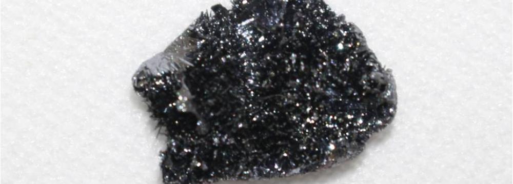
A research group at Canada's McGill University is using black phosphorus to present new generation of tiny transistors. The new study led by Dr. Thomas Szkopek and conducted by Iranian scientist Vahid Tayyari of McGill University suggests that black phosphorus could help researchers surmount one of the big challenges for future electronics—designing energy-efficient transistors.
The black phosphorus crystal structure is composed of puckered honeycomb layers with an interlayer distance of 0.5 nm. In 2004, researchers at the University of Manchester, UK, isolated and explored the remarkable properties of graphene, a one-atom-thick layer of carbon.
Since then, scientists have rushed to investigate a range of other 2D materials. One of those is black phosphorus that is similar to graphite and can be separated easily into single atomic layers, known as phosphorene. Black phosphorus is the second known elemental allotrope with a layered crystal structure that can be mechanically exfoliated to atomic layer thickness. Unlike graphite and graphene, black phosphorus is a semiconductor in both bulk and few-layer form.
“To lower the operating voltage of transistors, and thereby reduce the heat they generate, we have to get closer and closer to designing the transistor at the atomic level. The toolbox of the future for transistor designers will require a variety of atomic-layered materials: an ideal semiconductor, an ideal metal, and an ideal dielectric. All three components must be optimized for a well-designed transistor.
"Black phosphorus fills the semiconducting-material role,” said Dr. Szkopek, who is the senior author of the paper published in the journal Nature Communications. To examine how the electrons move in a phosphorus transistor, Dr. Szkopek and co-authors observed them under the influence of a magnetic field.
“What’s surprising in our results is that the electrons are able to be pulled into a sheet of charge which is two-dimensional, even though they occupy a volume that is several atomic layers in thickness.
“That finding is significant because it could potentially facilitate manufacturing the material, though at this point no one knows how to manufacture this material on a large scale.”


